⚛️ Majorana 1: Microsoft’s Quantum Leap
Welcome, AI & Semiconductor Investors,
Google is redefining cloud AI performance with its new A4X VMs—packing 72 Blackwell GPUs and 36 Grace CPUs into a powerhouse setup that promises a stunning leap in LLM training speed.
We’ll also delve into Microsoft’s next-level “Majorana 1” quantum chip and Lam Research’s 3D etch breakthroughs, both set to transform the future of computing—stay tuned!.… Let’s Begin
What The Chip Happened?
☁️ Clouded Vision: Google Launches Next-Gen A4X VMs
⚛️ Majorana 1: Microsoft’s Quantum Leap
⚙️ Lam’s 3D Revolution: New Tools, Bigger Targets
Read time: 7 minutes
Google (GOOGL)
☁️ Clouded Vision: Google Launches Next-Gen A4X VMs
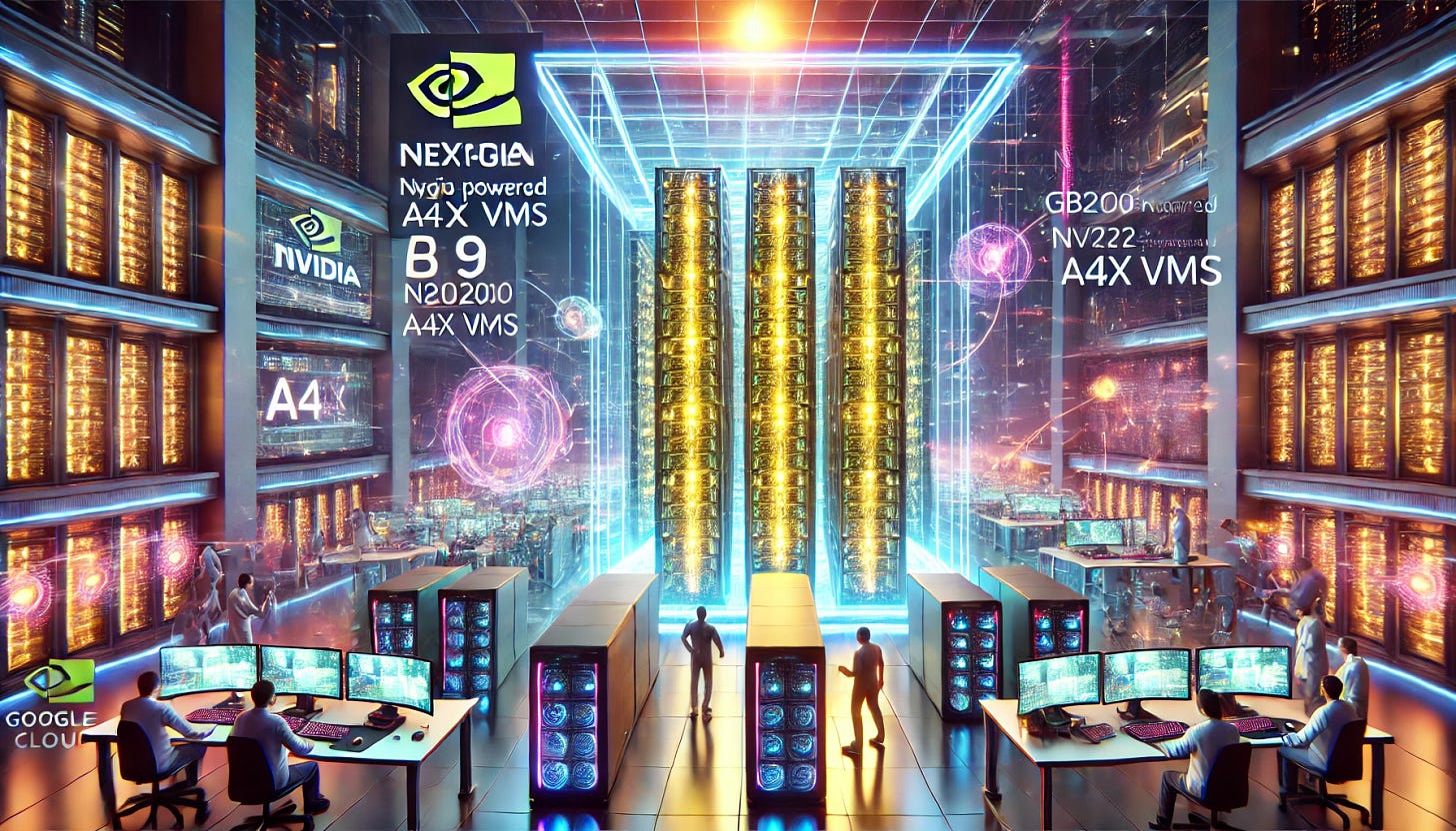
What The Chip: Google Cloud has become the first cloud provider to offer both the NVIDIA B200-powered A4 VMs and the NVIDIA GB200 NVL72-powered A4X VMs. This marks a major step forward in providing ultra-high-performance infrastructure designed for large language models and advanced AI workloads.
Details:
🏎️ A4X Redefines Speed: Each A4X VM supports NVIDIA GB200 NVL72 systems combining 72 Blackwell GPUs with 36 Grace CPUs, delivering over 1 exaflop of performance. According to Google, that’s a 4X increase in LLM training speed compared to the previous A3 VMs.
🧠 Built for “Reasoning Models”: The architecture focuses on “chain-of-thought” approaches, supporting massive context windows and concurrency across a 72-GPU domain. This is especially helpful for AI tasks that demand real-time, critical thinking.
♻️ New Liquid Cooling: Google’s third-generation liquid cooling prevents throttling under heavy loads and enables stable performance, part of what they call their AI Hypercomputer architecture.
🏗️ Flexible Scalability: With tens of thousands of GPUs in non-blocking clusters, large-scale training becomes more accessible. NVIDIA’s Alexis Bjorlin says this partnership aims to “tackle the most demanding generative AI, LLM, and scientific computing workloads.”
☁️ Integration Across Cloud Services: A4X VMs plug into GKE for containerized deployments and Vertex AI for managed model development, and Magic’s CEO says the new system “greatly improve[s] inference and training efficiency for our models.”
⚖️ Difference vs. A4 (B200) VMs: A4X suits large-scale, high-concurrency reasoning tasks, while A4 remains a versatile workhorse. For less massive training or serving, B200-based A4 VMs might still be cost-effective.
⚠️ Consider Costs & Complexity: Operating top-of-the-line GPUs can mean higher expenses. Investors should weigh the performance gains against potential increases in infrastructure and talent requirements.
Why AI/Semiconductor Investors Should Care: Google’s dual-offering puts it in a stronger competitive position against other cloud vendors, particularly for enterprises seeking high-end AI performance. By showcasing these next-gen VMs, Google is signaling that advanced AI infrastructure is vital for capturing AI market share and revenue growth—an important indicator for anyone investing in the future of data-centric computing.
Moore Semiconductor Investing
📗 [NEW!!] Unlock Q4 Semiconductor Earnings --- 60% OFF (NEW EARNINGS)
What The Chip: Get a front-row seat to the financials shaping the semiconductor industry. This continuously updated e-book by Jose Najarro distills the latest Q4 quarterly insights—from wafer production trends to AI chip breakthroughs—into a single comprehensive resource.
Details:
🔵 Dynamic Updates: Start with giants like TSMC and ASML, then expand to 30+ companies as their Q4 2024 earnings roll in. Earnings are restarting!!
🔵 Broad Coverage: From traditional chipmakers to cutting-edge AI semiconductor players, get the full picture as it emerges.
Why AI/Semiconductor Investors Should Care: This evolving earnings handbook gives you a strategic edge. Understanding quarterly earnings data is crucial for gauging industry health, discovering new growth leaders, and aligning your investment approach with emerging technological waves.
Disclaimer: For educational and informational purposes only. Not financial advice. Consult with a qualified professional before making any investment decisions. Updates are only for the Quarter of Earnings.
Microsoft (MSFT)
⚛️ Majorana 1: Microsoft’s Quantum Leap
What The Chip: Microsoft just unveiled “Majorana 1,” a quantum chip built on a new Topological Core architecture. The company believes it can compress decades of quantum progress into mere years, aiming for million-qubit systems that can handle real industrial and societal challenges.
Details:
⚛️ Topoconductor Breakthrough: Microsoft introduced a novel “topoconductor” material that can control Majorana particles, forming more stable and scalable qubits. “We took a step back and said ‘OK, let’s invent the transistor for the quantum age,’” said Chetan Nayak, Microsoft Technical Fellow.
🏗️ Million-Qubit Vision: The Majorana 1’s unique architecture purportedly paves the way to fit a million qubits on a single chip. “Whatever you’re doing in the quantum space needs to have a path to a million qubits,” Nayak added.
❄️ Digital Control at Scale: Microsoft’s new measurement approach relies on voltage pulses (like switching a light on and off), rather than finetuning analog dials. This simplifies the control mechanics—key for commercial feasibility.
⚙️ DARPA Endorsement: Microsoft’s inclusion in DARPA’s Underexplored Systems for Utility-Scale Quantum Computing program underscores its potential to deliver a usable million-qubit machine.
📏 Palm-Sized Chip: Despite aiming for massive qubit counts, Majorana 1 itself is compact, fitting in the palm of a hand for easy integration into data centers.
♾️ Industrial-Scale Potential: By simulating chemistry at the quantum level, Microsoft envisions breakthroughs like self-healing materials or microplastic breakdown catalysts. “Any company that makes anything could just design it perfectly the first time out,” said Matthias Troyer, Microsoft Technical Fellow.
💡 Atom-by-Atom Fabrication: The company painstakingly “sprays” indium arsenide and aluminum to create an exotic topological state, tackling one of the biggest engineering hurdles in quantum research.
Why AI/Semiconductor Investors Should Care: Quantum computing’s potential to solve massive industrial challenges—combined with the ongoing AI revolution—represents a substantial market opportunity. Microsoft’s topological approach might accelerate the timeline to functional, large-scale quantum systems, impacting everything from healthcare innovation to climate change solutions. For investors, it underscores a disruptive hardware leap that could reshape computing’s future.
Lam Research (LRCX)
⚙️ Lam’s 3D Revolution: New Tools, Bigger Targets
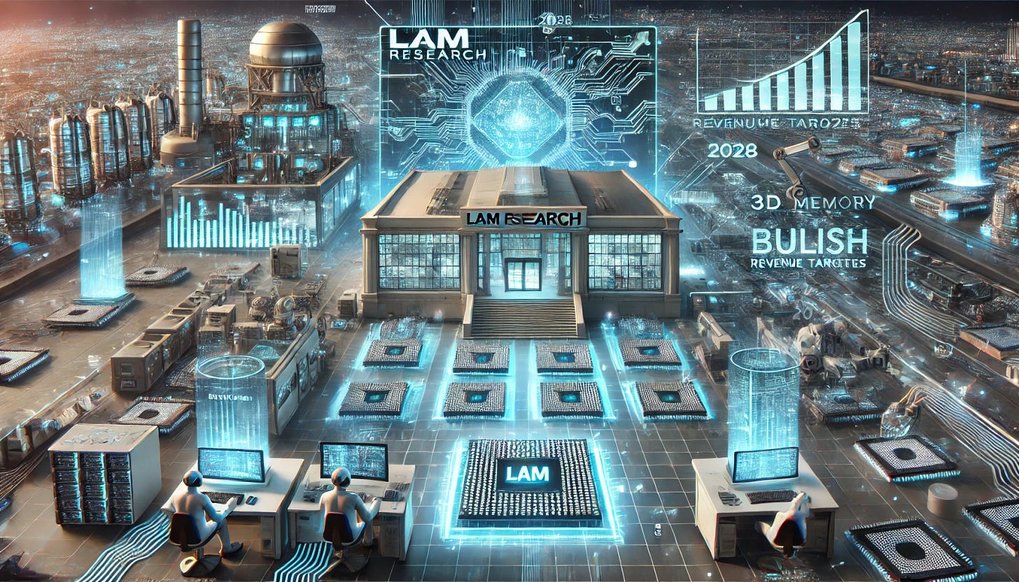
What The Chip: Lam Research just shared major breakthroughs at its Investor Day, revealing new etch and deposition products plus bullish revenue targets for 2028. CEO Tim Archer and his team spotlighted how 3D memory and advanced logic transitions are driving a boom in Lam’s served market expansion.
Details:
⚙️ Next-Gen Tools: Lam unveiled the “Akara” conductor etch system and an ALD moly product that replaces tungsten. According to Sesha Varadarajan (SVP, Global Products), these innovations promise “generational leaps” in performance for NAND, DRAM, and foundry/logic.
💾 3D NAND & DRAM: Over two-thirds of NAND capacity is still under 200 layers, setting up a big upgrade cycle. “We see customers needing to spend over $40B upgrading existing capacity,” said Archer.
🌏 Manufacturing Footprint: CFO Doug Bettinger highlighted Malaysia as Lam’s largest factory, enabling lower costs and fueling a push toward 50%+ gross margins.
🤖 Collaborative Robots: The newly introduced “Dextro” cobot automates critical maintenance steps. “Precision service is key to boosting uptime,” Archer explained.
💸 Financial Outlook: By 2028, Lam expects $25B to $27B in revenue, ~50% gross margins, and $6+\ in EPS. Bettinger added, “We’re leveraging the biggest share of new inflections to outpace WFE growth.”
Why AI/Semiconductor Investors Should Care: Lam’s advanced etch and deposition solutions lie at the heart of 3D architectures powering next-gen AI applications. As chipmakers push further into vertical scaling, Lam’s tools become increasingly critical. Add in a fast-growing installed base services business, and Lam’s latest moves position the company for strong profitability and market leadership in an era of trillion-dollar semiconductors.
Youtube Channel - Jose Najarro Stocks
[NEW] Semiconductor Q4 Earnings Book — 60% OFF
X Account - @_Josenajarro
Disclaimer: This article is intended for educational and informational purposes only and should not be construed as investment advice. Always conduct your own research and consult with a qualified financial advisor before making any investment decisions.
The overview above provides key insights every investor should know, but subscribing to the premium tier unlocks deeper analysis to support your Semiconductor, AI, and Software journey. Behind the paywall, you’ll gain access to in-depth breakdowns of earnings reports, keynotes, and investor conferences across semiconductor, AI, and software companies. With multiple deep dives published weekly, it’s the ultimate resource for staying ahead in the market. Support the newsletter and elevate your investing expertise—subscribe today!
[Paid Subscribers] Lam Research Charts a Path to Higher Growth — 2/20/25 Investor Day
Executive Summary
Lam Research, a leading provider of deposition and etch equipment for the semiconductor industry, recently hosted its much-anticipated Investor Day in New York City. Executives highlighted the company’s core strengths in memory (NAND and DRAM), foundry/logic, and customer support, revealing detailed roadmaps and quantitative guidance that extend well into the decade. In 2024, Lam achieved a record-high gross margin of 48.2% and delivered an operating margin above 30%, with total revenues of $16.2 billion. Tim Archer, Lam’s President and CEO, emphasized the significance of next-generation architectures such as 3D structures, gate-all-around (GAA), backside power distribution, and high-density NAND. Archer stated, “Lam has never been better positioned to outperform, and there is no better place to be in semi cap than Lam Research.”
Doug Bettinger, Executive Vice President and Chief Financial Officer, reinforced the company’s confidence by projecting revenues of $25–$27 billion by 2028, near 50% gross margin, and $6–$7 earnings per share (EPS). Bettinger also laid out a longer-range view for the time when the semiconductor industry reaches $1 trillion in annual sales, envisioning Lam’s revenue crossing $30 billion, with gross margins surpassing 50% and operating margins above 35%. Underlying these targets is the expectation that Lam’s installed base and service business, which the company calls its Customer Support Business Group (CSBG), will outgrow the broader wafer fabrication equipment (WFE) market.
Growth Opportunities
Expanding Memory Technologies
A key focus is the anticipated conversion of “2/3 of the industry’s bit capacity” in NAND, still below 200 layers, up to 200 layers and beyond. According to Tim Archer, these technology upgrades represent “over $40 billion” of investment in equipment as customers pursue higher-layer NAND devices. While overall NAND WFE may remain below prior peaks, Lam expects to capture a larger fraction of this spending because high-aspect-ratio etch steps and 3D-related deposition steps grow disproportionately with each incremental layer.


